Project
There are two ways to wire single-key PCBs:
- Short wires: Cut small wires between each PCB. Requires the optional row/column connections.
- One long wire: Use a single wire for every row/column. Requires a bare wire or the insulation removed at every PCB.
Between these I've found #2 to be neater and faster, so I recommend you wire Plum Twists with it. That's what I'll cover from here on out.
Supplies
For wiring you'll need wire, wire strippers, a knife and a self-healing mat to cut on. The knife is handy for cleaning up the 3D print and stripping wire, and the self-healing mat is a great cutting surface and you can use it to keep your work table clean when soldering too. Your local art supply store will surely have both of these, and you should go buy from them and support them! You can also easily find them online.
You'll also of course need a soldering iron and solder. Something affordable like the Pinecil or TS100 will do the job just fine, and because of the large row and column pads, you can use a large tip like the BC2 tip the Pinecil comes with.
I recommend solid 26-30 gauge wire. Solid means there's only one conductor inside. Some flexible wires are stranded and have many twisted conductors inside (much like braided hair), which make the end of the wire harder to solder. I recommend buying a pack of multiple colors of insulated wire. You'll need insulated wire to solder the rows, but you could substitute uninsulated wire for the columns. Nevertheless, the insulated wire is safer as there's no chance of accidentally shorting something.
Twisting
I include a large paperclip in all Plum Twist orders I receive online. I highly recommend you use it for twisting in the PCB! Fully unbend the paperclip so it becomes a straight line, then fold it exactly in half. You can then stick the 2 ends of the paperclip into the 2 small holes on the PCB's centerline to get a better grip when twisting.

If you have a 3D printer, you can make the process even easier for yourself. I've designed a 3D model that keeps your paperclip ends aligned and makes the jig easier to grip. It should take about 30 minutes to print and doesn't need supports.
Instructions
- Fit check! Before you start wiring, I recommend you make sure that all the PCBs twist into the keyboard. After 3D printing there will sometimes be chunks of support you've forgotten stuck inside the sockets, and you'll need to cut these out to make the PCB twist in smoothly. It's much easier to fix these issues before you start wiring.
- Measure a wire for a row or column. You want to have enough to reach from the microcontroller
to the first key and all the way to the last key, plus about 5–10 centimers (2–4 inches) of
extra for slack and mistakes.
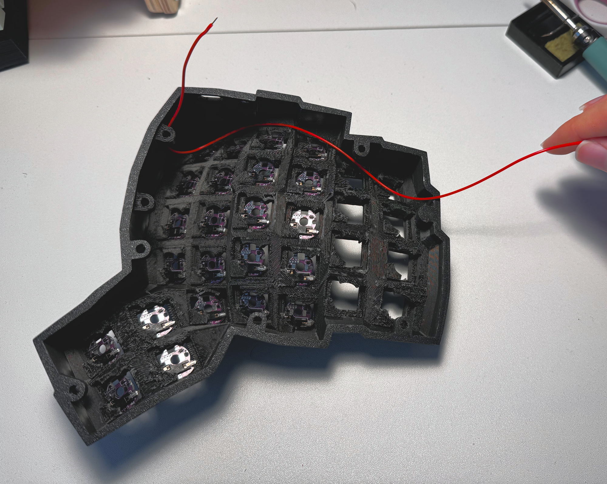
- Strip the end of the wire about 2mm. This end will be soldered to the last key from the microcontroller in the row/column.
- Using the grid on your mat, measure 3cm (3 gridlines) from where you've stripped the wire. Use your wire strippers to make two cuts into the insulation, about 5mm apart.
- Repeat this step for every key that's left. You should space cuts by 3cm for keys right next to each other, but space them further apart if the keys are spread out.
- Use a knife blade to remove the insulation between each pair of cuts. I find it easiest to try
to dig in with the blade first, then cut.
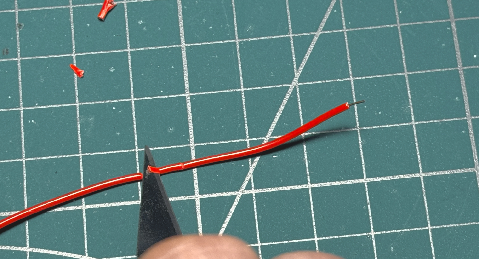
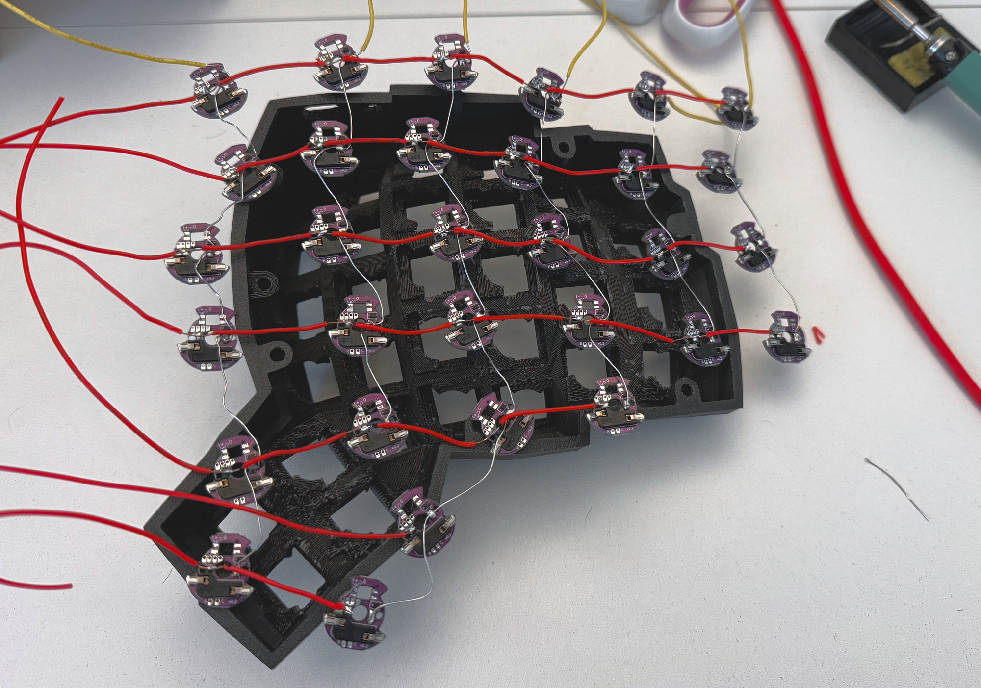
- Once you've made some wires, you can start soldering them to the PCBs. I recommend you solder
the matrix outside of the case first, then try twisting the PCBs in after you've soldered
everything. I also find I get the best results by pre-tinning the wire (applying some solder to
it) before soldering it to the PCB. It's easiest to solder the columns first, and to solder the
column wire horizontally through the PCB, with the wire entering the right side and leaving the
left. However, make sure the wire clears the holes to the side of the pads, through which the
switch pins are inserted (solder vertically instead of horizontally if the wire doesn't clear).
Solder the rows after the columns are finished as the wire naturally lines up. Make sure to use
plenty of solder so that you have a good connection!
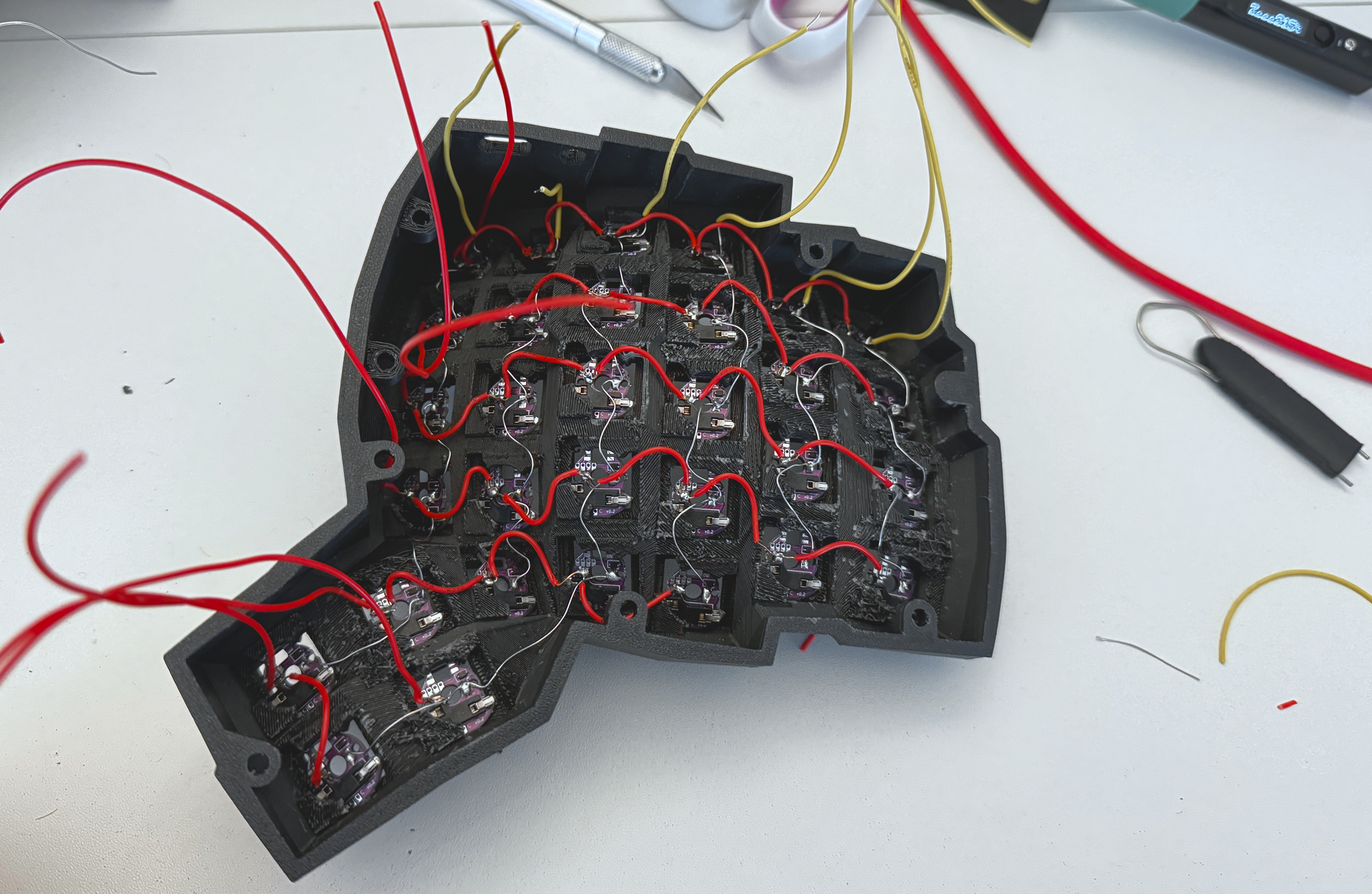
- When you're done, place the matrix in the keyboard and twist in all the PCBs. Then gather the
ends of wire and measure how much wire is needed to reach the microcontroller. Cut off any
excess.
- For wiring the microcontroller, encoders, etc as well as programming. I recommend you check out the Cosmos wiring & programming guide. In QMK you should set your diode direction as ROW2COL.
RGB LEDs
If you take one thing away from this next paragraph, remember: chain the inputs and outputs (I's and O's). Collect the powers and grounds (+'s and -'s).
Every LED must have its Ground (-) pin connected to one of the ground pins on the microcontroller. The Power Pins (+) should be run to the 5V/VUSB pin on microcontrollers with 5V logic (e.g. ATmega32U4-based ones), whereas it should be run to the 3.3V pin on microcontrollers with 3.3V logic (e.g. RP2040). It is techically against the spec to supply these LEDs with only 3.3V, but I have seen this work well enough to feel comfortable recommending you do so. The alternative is to power the LEDs from 5V but stick a “sacrificial LED” in between the first PCB and your 3.3V microcontroller to boost the signal voltages.
To go about soldering every PCB's + and - pins to 2 single pins on the microcontroller, I suggest you use a "tree branch" approach. Cut 6 or so wires to about 3in / 8cm, strip both ends, and solder these wires to + pins of a cluster of neighboring PCBs. Then twist together all the loose ends. Repeat this process for the rest of the PCBs, so that you have about 6 bundles of 6 wires. Now cut more wires and solder a wire to the end of every bundle. Finally, twist these wires together and connect them to microcontroller pin. Repeat this process for the - pins. If you have thicker wires, you may find creating bundles of 4 and doing 3 rounds of bundling/twisting/soldering to be easier. If you like being neat, you can bundle together the columns first, then connect together all the column power pins.
If you have a programming or math background, you may appreciate that with a branching factor of k, the number of solder joints per PCB for say the + pins is at most k/(k-1) for a full tree. Compare that to a factor of 2 for the conventional wiring used on Amoeba PCBs. It may look unconventional but it saves you time!
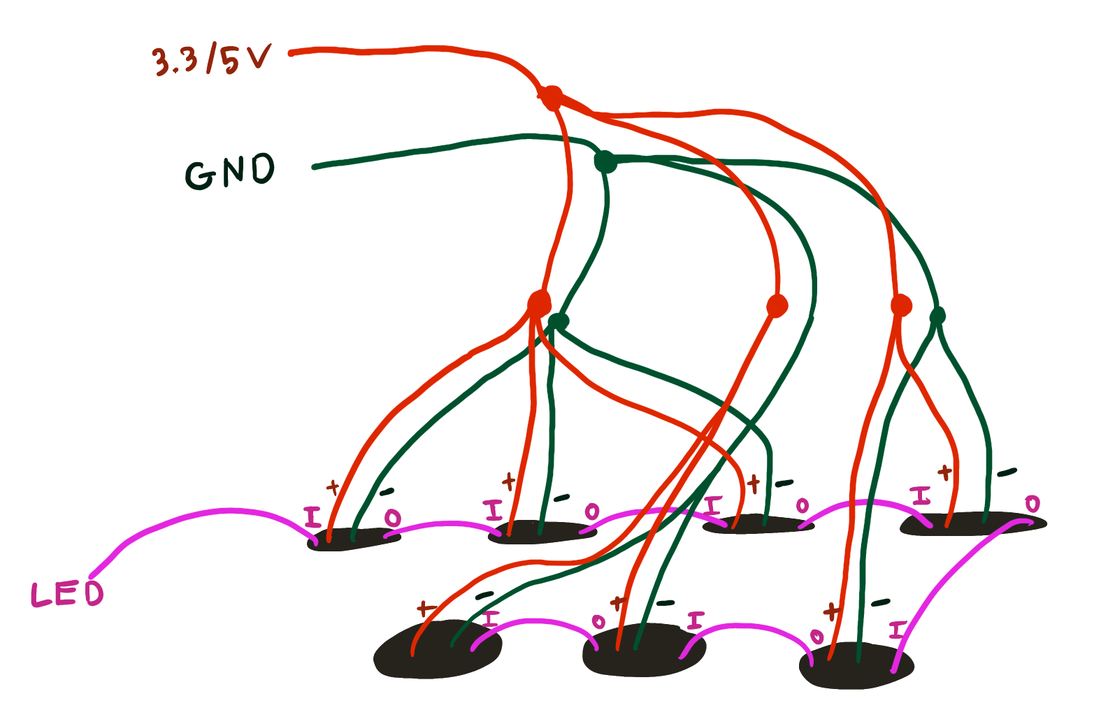
For the Input (I) and Output (O) connections, the Input of the PCB nearest to the microcontroller should connect to a microcontroller pin. After that, connect all PCBs in a chain (a zigzap pattern is easiest) so that the Output of every PCB connects to the Input of the next. The final PCB should have its Output (O) not connected to anything.
PCB Layout
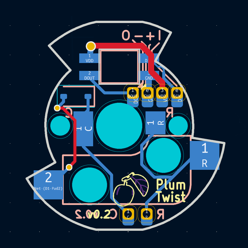
This image is looking at the top (flat side) down. If you're looking at the PCB from the hotswap/pad side, mentally mirror everything horizontally.
Open Source
You can find design files for the PCB over at the Cosmos Keyboard PCBs repository.